Ultra-fine resolution manufacturing represents the frontier where physics, engineering, and materials science converge to create structures at scales that challenge our fundamental understanding of precision.
🔬 The Nanoscale Revolution in Modern Manufacturing
Manufacturing at the edge of physical limitations has transformed from a theoretical curiosity into a commercial necessity. Today’s semiconductor chips, medical devices, and optical components demand features measured in nanometers—dimensions where traditional manufacturing paradigms break down completely. This shift toward ultra-fine resolution manufacturing isn’t merely about making things smaller; it’s about reimagining entire production processes to account for quantum effects, atomic-scale surface interactions, and the probabilistic nature of matter itself.
The journey toward extreme precision began decades ago with the semiconductor industry’s relentless pursuit of Moore’s Law. What started as micron-scale features has progressed to transistors measuring just 3 nanometers in width—roughly 15 silicon atoms across. This progression hasn’t been linear or easy; each reduction in feature size has required overcoming fundamental physical barriers that once seemed insurmountable.
Breaking Through Traditional Manufacturing Limits
Conventional manufacturing techniques like milling, drilling, and casting operate comfortably at scales measured in millimeters or micrometers. However, these methods encounter hard limits when attempting to create features below approximately 10 micrometers. At this threshold, tool wear, material properties, and thermal effects become dominant factors that overwhelm precision efforts.
The transition to ultra-fine resolution demands entirely different approaches. Photolithography, electron beam lithography, focused ion beam milling, and atomic layer deposition represent the new toolkit. Each technique manipulates matter using energy rather than mechanical force, allowing manufacturers to pattern materials with precision that would be impossible with physical tools.
The Physics of Extreme Precision
At nanometer scales, the familiar rules of classical physics give way to quantum mechanical effects. Electrons begin to tunnel through barriers that should theoretically contain them. Surface tension and van der Waals forces become dominant, affecting how materials stick together or resist separation. Even the concept of a clean, sharp edge becomes fuzzy when features approach atomic dimensions.
Temperature control emerges as a critical challenge. Thermal expansion coefficients that are negligible at macro scales become significant sources of error when working with nanometer tolerances. A temperature variation of just one degree Celsius can cause dimensional changes that completely destroy precision at these scales. Manufacturing facilities targeting ultra-fine resolution often maintain environmental conditions more stable than those in spacecraft.
⚙️ Technologies Enabling Ultra-Fine Manufacturing
The arsenal of techniques available for ultra-fine resolution manufacturing continues to expand, each with distinct advantages and limitations. Understanding these technologies reveals both the current state of the art and the boundaries we’re pushing against.
Extreme Ultraviolet Lithography: Printing with Light at the Edge
Extreme ultraviolet lithography (EUV) represents perhaps the most significant recent breakthrough in semiconductor manufacturing. Using light with a wavelength of just 13.5 nanometers—compared to 193 nanometers for previous-generation systems—EUV enables the creation of features smaller than the wavelength of visible light.
The technology required decades of development and billions in investment. EUV systems must operate in near-perfect vacuum conditions because air absorbs the extreme ultraviolet radiation. The mirrors used to focus the light must be polished to within a fraction of an atomic layer, making them among the smoothest objects ever created. Despite these challenges, EUV has become indispensable for manufacturing the most advanced processors and memory chips.
Electron and Ion Beam Techniques
When photons prove too large, charged particles offer an alternative. Electron beam lithography can pattern features with resolution below one nanometer by scanning a focused electron beam across a substrate. The technique provides exceptional precision but suffers from relatively slow throughput, making it ideal for prototyping and mask making but less suitable for high-volume production.
Focused ion beam systems take a different approach, using heavy ions to physically remove material atom by atom. This subtractive process enables three-dimensional sculpting at nanometer scales, creating structures impossible to achieve through additive or photographic methods. The precision comes with a cost—ion beams can damage surrounding material, requiring careful optimization of beam parameters and processing conditions.
Material Challenges at the Frontier
As feature sizes shrink, materials themselves begin to behave differently. Bulk material properties no longer accurately predict behavior when structures contain only hundreds or thousands of atoms. This reality forces manufacturers to reconsider fundamental assumptions about material selection and processing.
Size-Dependent Material Properties
Gold, for example, is famously inert and non-reactive at normal scales. However, gold nanoparticles smaller than 5 nanometers become excellent catalysts. Silicon transitions from an indirect to direct bandgap semiconductor when formed into quantum dots, changing its optical properties dramatically. These size-dependent effects can be advantageous when properly controlled but represent significant challenges for maintaining consistent manufacturing outcomes.
Surface-to-volume ratios skyrocket at nanoscales, making surface properties dominant over bulk characteristics. Contamination that would be insignificant in traditional manufacturing can completely alter the performance of nanostructured devices. A single atomic layer of oxide on a metal contact can increase electrical resistance by orders of magnitude. Maintaining cleanliness becomes paramount, requiring ultra-high vacuum conditions and sophisticated surface preparation protocols.
📐 Metrology: Measuring the Immeasurable
Perhaps the most fundamental challenge in ultra-fine resolution manufacturing isn’t making small things—it’s verifying that you made what you intended. Measurement and inspection at nanometer scales requires techniques as sophisticated as the manufacturing processes themselves.
When Light Becomes Too Crude
Optical microscopes hit fundamental resolution limits around 200 nanometers due to light diffraction. This limitation, described by Ernst Abbe in the 1870s, means that light-based inspection simply cannot resolve features in modern advanced semiconductors. Manufacturers have turned to scanning electron microscopes, atomic force microscopes, and X-ray scattering techniques to fill the metrology gap.
Each metrology technique introduces its own challenges. Electron microscopy provides excellent resolution but can damage sensitive samples. Atomic force microscopy offers true three-dimensional surface mapping but suffers from slow scan speeds and tip wear. X-ray techniques enable non-destructive subsurface imaging but require complex data interpretation. No single method solves all measurement needs, forcing manufacturers to deploy multiple complementary techniques.
Statistical Quality Control in Probabilistic Domains
Traditional manufacturing quality control relies on deterministic processes where identical inputs produce identical outputs. Ultra-fine resolution manufacturing operates in a more probabilistic realm where quantum effects, atomic-scale variations, and stochastic processes introduce inherent variability.
This reality demands new statistical frameworks. Rather than specifying exact dimensions, manufacturers increasingly work with probability distributions and yield models. A process might be considered successful if 95% of devices meet specifications, with the understanding that perfect uniformity is physically impossible at these scales. This shift requires sophisticated modeling capabilities and real-time process adjustment to maintain yields within acceptable bounds.
🌡️ Environmental and Stability Requirements
The extreme precision of ultra-fine resolution manufacturing demands unprecedented control over the manufacturing environment. Factors that are completely negligible in conventional factories become dominant sources of error.
Vibration Isolation at the Angstrom Level
A person walking past a machine can generate floor vibrations that propagate through building structures. At macro scales, these vibrations are insignificant. For nanometer-precision equipment, they represent catastrophic disturbances. Advanced manufacturing facilities employ sophisticated vibration isolation systems, including pneumatic tables, active damping systems, and in some cases, entire buildings mounted on springs.
The most sensitive equipment may be located in sub-basements resting on bedrock, isolated from upper floors where human activity occurs. Some facilities even monitor seismic activity and pause operations during minor earthquakes that would go unnoticed by building occupants. The level of isolation required rivals that of gravitational wave detectors, though for different reasons.
Atmospheric Control and Contamination
Modern cleanrooms maintain particle counts orders of magnitude below outdoor air, but ultra-fine manufacturing pushes beyond even these stringent standards. A Class 1 cleanroom allows fewer than one particle larger than 0.5 micrometers per cubic foot of air. Some advanced processes require Class 0.1 or better, approaching the fundamental limit where individual molecules become the concern.
Chemical contamination presents equal challenges. Airborne molecular contaminants—organic compounds outgassing from materials, trace acids, or bases—can react with sensitive surfaces at the molecular level. Manufacturing spaces employ sophisticated filtration systems using activated carbon, chemical scrubbers, and continuous air exchange to maintain atmospheric purity that exceeds that of many scientific laboratories.
Economic Realities and the Cost of Precision
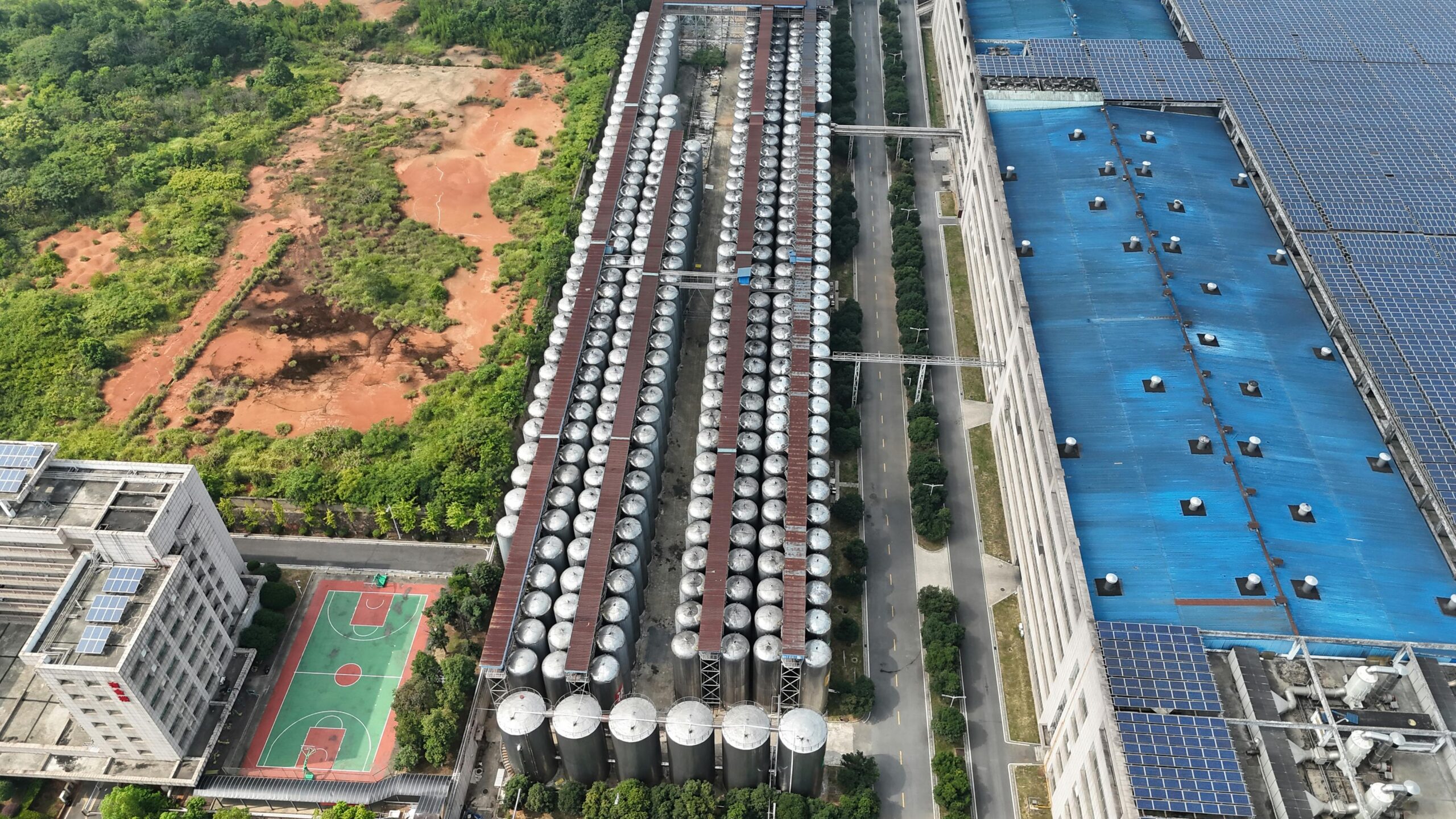
Pushing precision to the edge carries enormous economic implications. The semiconductor industry provides the clearest example: a modern advanced fabrication facility costs between $15 billion and $20 billion to construct. A single EUV lithography tool costs approximately $150 million. These staggering investments are justified only by high-value applications where ultra-fine resolution provides irreplaceable advantages.
The Democratization Challenge
As manufacturing capabilities advance, a concerning gap emerges between leading-edge facilities and the broader manufacturing ecosystem. Only a handful of companies worldwide can afford to build and operate factories capable of producing the most advanced semiconductor nodes. This concentration raises questions about supply chain resilience, technological access, and innovation barriers.
Efforts to democratize ultra-fine manufacturing focus on shared facilities, university cleanrooms, and emerging techniques that might reduce capital intensity. Two-photon polymerization 3D printing, for instance, can create three-dimensional structures with sub-micrometer resolution using equipment that fits on a laboratory bench. While not matching the most advanced semiconductor fabrication, such technologies extend precision manufacturing capabilities to smaller organizations and researchers.
🚀 Emerging Frontiers and Future Directions
Even as manufacturers push current techniques to their limits, researchers explore fundamentally new approaches that might enable the next leap in precision. These emerging technologies operate at the boundary between manufacturing and atomic-scale manipulation.
Atomic Layer Manufacturing
Atomic layer deposition already enables the growth of films with single-atomic-layer thickness control. Researchers now work to extend this precision to lateral dimensions, enabling true atomic-level manufacturing. Techniques like atomic layer etching remove material one atomic layer at a time with molecular-scale selectivity. The combination promises manufacturing processes where every atom occupies its intended position.
DNA origami represents a biomolecular approach to atomic-scale assembly. By designing specific DNA sequences, researchers create self-assembling structures with nanometer precision. These biological templates can guide the placement of nanoparticles, proteins, or other functional elements, potentially enabling manufacturing paradigms where molecular self-assembly replaces top-down fabrication techniques.
Quantum Technologies as Both Challenge and Opportunity
Quantum computing devices represent perhaps the ultimate expression of ultra-fine manufacturing requirements. Superconducting qubits require fabrication precision that maintains quantum coherence, where even subtle defects or contamination can destroy fragile quantum states. Manufacturing these devices pushes every aspect of precision fabrication to its limits.
Paradoxically, quantum effects that complicate conventional manufacturing might enable new capabilities. Quantum sensors can detect magnetic fields, gravity gradients, or time variations with unprecedented sensitivity, potentially revolutionizing metrology and process control. Quantum-enhanced lithography might surpass classical resolution limits through entangled photon states. The quantum realm presents both obstacles and opportunities for future manufacturing advancement.
Cross-Industry Applications and Impact
While semiconductors drive much ultra-fine manufacturing development, applications span diverse industries. Medical devices benefit from micro- and nano-scale features that interact with individual cells or precisely deliver drugs. Optical metamaterials with subwavelength structures enable capabilities impossible with conventional optics, from perfect lenses to invisibility cloaking.
Energy technologies increasingly rely on nanostructured materials. Solar cells with precisely engineered surface textures capture light more efficiently. Battery electrodes with controlled nanoporosity enable faster charging and higher capacity. Catalysts with maximized surface area and optimized active sites improve efficiency in everything from automotive emissions control to industrial chemical production.
The Human Element in Extreme Precision
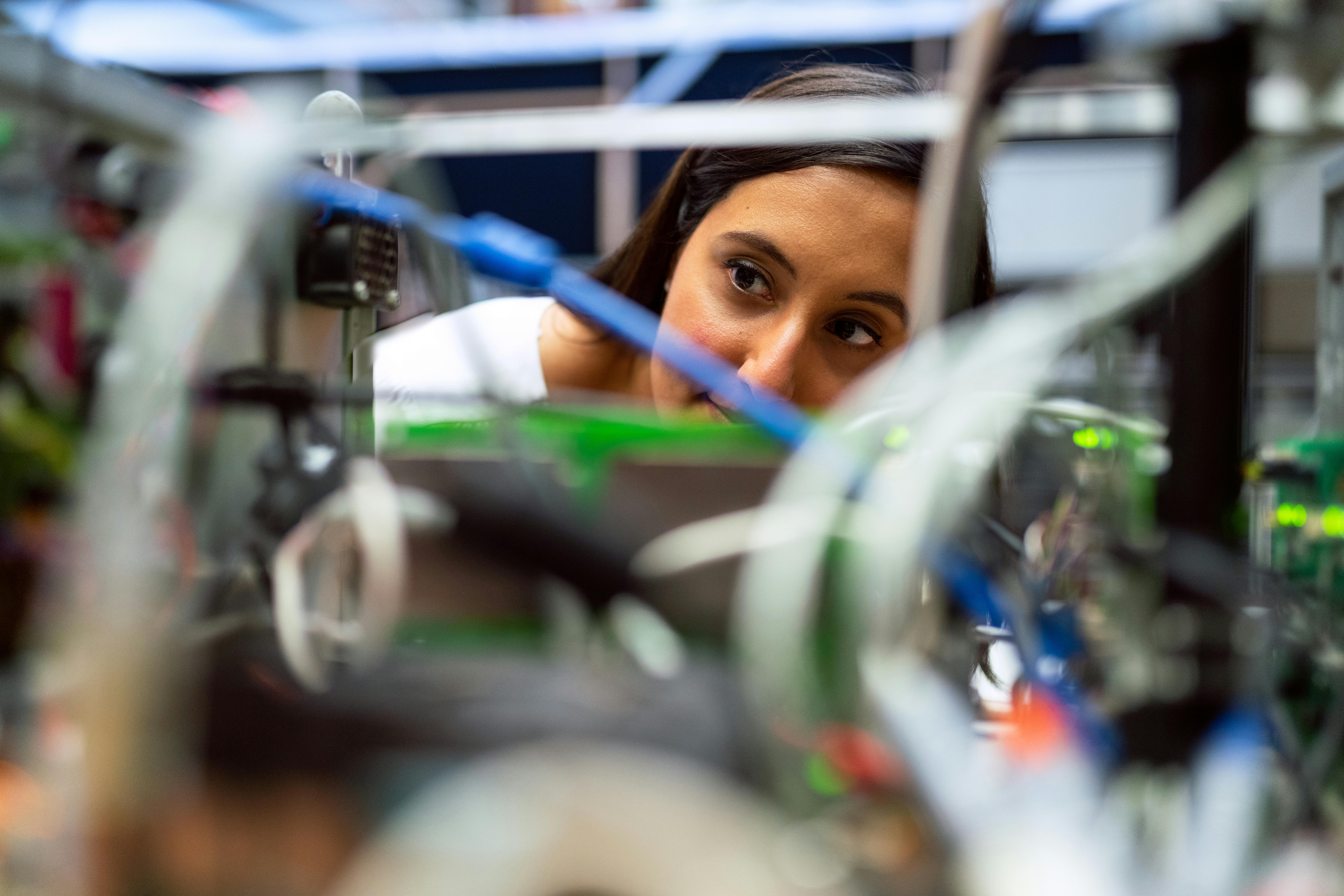
Despite advancing automation, human expertise remains central to ultra-fine manufacturing. Process engineers develop the sophisticated recipes that transform raw materials into functional devices. Metrology specialists interpret complex measurement data to identify process variations. Maintenance technicians keep extraordinarily sensitive equipment operating within specification.
Training the workforce for extreme precision manufacturing presents unique challenges. Traditional apprenticeship models struggle when processes operate at scales invisible to human senses. Sophisticated simulation tools and virtual reality training environments help bridge the gap, allowing workers to visualize and interact with nanoscale processes that they can never directly observe.
🎯 Navigating the Boundaries of Physical Law
Ultra-fine resolution manufacturing ultimately confronts fundamental physical limits. The Heisenberg uncertainty principle places hard boundaries on simultaneous position and momentum knowledge. Thermal fluctuations provide an energy floor that cannot be eliminated at non-zero temperatures. Quantum tunneling ensures that perfect confinement becomes impossible below certain length scales.
These aren’t engineering challenges to be overcome with better equipment—they’re fundamental features of physical reality. The final frontier of manufacturing precision involves learning to work within these constraints rather than fighting against them. Future advances may come less from pushing smaller and more from cleverly exploiting quantum effects, designing for manufacturability at atomic scales, and accepting probabilistic rather than deterministic outcomes.
The journey toward ultimate precision continues to reveal new challenges and possibilities. Each boundary overcome exposes new frontiers, each limitation circumvented reveals additional constraints. This ongoing exploration drives technological progress, economic value creation, and deepening scientific understanding. As we push precision to the edge, we simultaneously expand the edge itself, discovering that the frontier of what’s possible extends further than we imagined—constrained ultimately only by the fundamental laws governing our universe.